

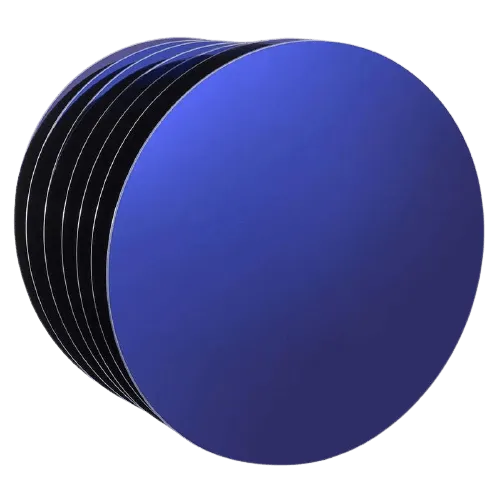
If you're sourcing soi wafer 販売 or any 4-inch semiconductor substrate, getting the dimensions and tolerances right before you order saves costly re-spins and delays. Soka Technology stocks a broad range of wafer types, from standard silicon substrates to compound and sapphire options, all available with verified specs. Here is what every buyer needs to know.
Understanding the dimension of 4inch wafer: Core Specs
The dimension of 4inch wafer is not simply "100 mm diameter." Industry standards define a full set of controlled parameters:
- Diameter: 100 mm nominal, with a typical tolerance of ±0.5 mm
- Thickness: Varies by material and resistivity grade; standard silicon runs 525 µm, but check the datasheet for your specific order
- Total Thickness Variation (TTV): Critical for lithography; premium grades hold TTV below 2 µm
- Bow and Warp: Bow is the deviation of the median surface from a reference plane; warp is peak-to-valley across the full wafer. Both must be within spec for chuck-based processing
- Flat or Notch: 4-inch wafers typically carry a primary flat (SEMI standard) for orientation; confirm flat length before ordering
- Edge Profile: Rounded (R-edge) or chamfered profiles affect handling yield in automated cassette systems
The 100/0.001 listing at Soka Technology is a good reference point for understanding how resistivity notation (orientation/resistivity in Ω·cm) is encoded directly in the product name. Always cross-reference that notation with the full spec sheet.
Silicon Substrate Types and Surface Finish Choices
The silicon substrate is the workhorse of the catalog. Soka Technology offers several silicon substrate types distinguished by:
- Orientation: (100), (111), and (110) crystal cuts serve different device architectures
- Dopant and resistivity: P-type (boron) and N-type (phosphorus/antimony) grades span intrinsic to heavily doped ranges
- Surface finish: Single-side polished (SSP) is standard; double side polishing delivers tighter flatness and is mandatory for through-wafer optical or via applications
- Epitaxial-ready: Some lots are epi-polished for direct layer growth without additional prep
For applications needing enhanced surface functionality, silver-coated silicon wafers add a metallic thin film to the polished face, useful in SERS, photonics, and sensor work. If you need pre-diced pieces rather than full rounds, silver silicone chips provide the same coating on singulated substrates, reducing in-house dicing costs.
soi wafer 販売: Why SOI Dimensions Demand Extra Attention
soi wafer 販売 (Silicon-On-Insulator) introduces two additional critical dimensions that bulk silicon does not have:
- Device layer thickness: Typically measured in nanometers to low microns; uniformity across the wafer face directly affects transistor threshold voltage
- Buried oxide (BOX) thickness: Ranges from tens of nanometers (ultra-thin BOX) to several microns; affects capacitance and RF isolation
- Handle wafer thickness: Standard 525 µm for 4-inch, but thinned handle options exist
When evaluating soi wafer 販売, always request the device layer uniformity map (typically expressed as mean ± sigma in nm) alongside the standard dimensional certificate. A wafer that passes bow/warp but has poor device layer uniformity will still fail in FD-SOI or MEMS applications.
You can check the latest price and grab the Soka Technology discount code before requesting a quote to maximize your per-unit savings, especially on multi-wafer lots.
Sapphire and Compound Wafer Options: Tolerances Compared
Not every application calls for silicon. Here is how the main alternative substrates compare on key 4-inch dimensional parameters:
| Substrate | Typical Thickness | TTV Target | Key Use Case |
|---|---|---|---|
| double side polished c sapphire | 430–650 µm | < 5 µm | GaN epi, optical windows |
| sapphire wafer (SSP) | 430–650 µm | < 10 µm | LED, RF, general epi |
| indium phosphide wafer | 350 µm (typical) | < 10 µm | III-V lasers, photonics |
| Silicon substrate (SSP) | 525 µm | < 5 µm | CMOS, MEMS, general |
A few points worth calling out:
- Sapphire wafer grades: C-plane (0001) is by far the most common for nitride growth; R-plane and M-plane are specialty orientations. Double side polishing on the double side polished c sapphire is essential when the substrate back-surface must also transmit or when bonding processes require a flat reference
- Indium phosphide wafers are III-V compound semiconductors with significantly higher fragility than silicon or sapphire; handle with dedicated InP cassettes and avoid contact with the polished face
- Sapphire wafer grades also differ in impurity levels; optical-grade material has stricter absorption specs than epi-grade
Shipping Fragile Wafers and Handling Notes
Regardless of which substrate you order, 4-inch wafers arrive in SEMI-standard cassettes or individual gel-paks. A few handling reminders:
- Inspect the outer packaging for shipping damage before opening the inner cassette
- Store wafers in a cleanroom or controlled environment immediately on receipt; particulate contamination on a polished face is difficult to reverse without re-polishing
- SOI and InP wafers are especially sensitive to thermal shock; allow packages to equilibrate to room temperature before opening in a cold lab
- Use vacuum wands or edge-grip tweezers; finger contact on any polished surface introduces organic contamination
For current availability, payment options, and to apply the site-wide savings, visit the Soka Technology discount code page where the latest offer is listed.
Requesting a Quote: What to Include
Soka Technology's product pages let you configure or inquire about custom specs. To speed up the process, have the following ready:
- Material and orientation (e.g., Si (100), C-plane sapphire, InP (100))
- Diameter and thickness (confirm whether standard or custom)
- Dopant type and resistivity range (for silicon and InP)
- Surface finish (SSP, DSP, epi-polished, coated)
- Device and BOX layer targets if ordering soi wafer 販売
- Quantity and delivery timeline (affects whether stock or custom-grown material is quoted)
- Certification requirements (lot traceability, COA, XRF for coated wafers)
Providing complete specs upfront avoids back-and-forth and reduces lead time, particularly for specialty materials like indium phosphide or silver-coated silicon wafers.
 Shopping at Soka Technology? See today's verified Soka Technology discount code
Frequently asked questions
What does the resistivity notation like 100/0.001 mean on a wafer listing?
The notation encodes the crystal orientation and resistivity in a single string. The first number refers to the crystal plane orientation (e.g., (100)) and the decimal value represents the resistivity in Ω·cm. Always verify this against the full datasheet before ordering to confirm dopant type and carrier concentration.
How does soi wafer 販売 differ from a standard silicon substrate in terms of dimensions?
An SOI wafer shares the same outer diameter and handle thickness as a bulk silicon substrate, but it adds two critical internal dimensions: the device layer thickness and the buried oxide (BOX) thickness. Both must be specified and verified for your application, as they directly affect electrical and mechanical performance.
Is double side polishing necessary for sapphire wafers used in LED epi growth?
Single-side polished sapphire is sufficient for most standard LED epi processes where only the front face is used. Double side polished c sapphire becomes important when the back surface must also be flat for bonding, through-wafer measurement, or optical transmission applications.
Can I order silver-coated silicon wafers in diced chip form instead of full rounds?
Yes. Soka Technology offers silver silicone chips, which are pre-diced substrates with the same silver coating as the full-round wafers. This is a practical option if you want to avoid in-house dicing and the associated risk of edge chipping or coating delamination.
How fragile are indium phosphide wafers compared to silicon during shipping?
Indium phosphide wafers are significantly more brittle than silicon and have a lower fracture toughness, making them prone to edge chipping and cleavage along crystal planes. They should be shipped and handled in dedicated InP-compatible cassettes, and packaging should be inspected carefully before opening after transit.
Is there a discount available when buying multiple wafer types from Soka Technology?
Soka Technology offers a sitewide discount code that applies across their product catalog. Check the current offer on the Soka Technology discount code page before placing your order to confirm the latest savings, especially useful when ordering multiple substrate types in one purchase.