

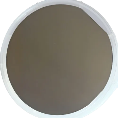
A silicon substrate is the default starting point for most semiconductor work, but sapphire often wins in high-frequency, optical, and high-temperature environments. Understanding the trade-offs up front saves you from costly re-spins later. This guide walks through every decision point so you can order with confidence from Soka Technology.
What Makes a Silicon Substrate Different From Sapphire
Silicon and sapphire are both single-crystal materials, but they serve different masters.
Silicon substrates are the workhorse of the industry. They are abundant, affordable, available in a wide range of dopant levels and orientations (think 100/0.001 resistivity grades), and compatible with the broadest set of fab processes. If you are building CMOS logic, power devices, or MEMS sensors, silicon is almost always the right call.
Sapphire substrates are electrically insulating, optically transparent from UV through mid-IR, and chemically inert at high temperatures. They are the substrate of choice for GaN-on-sapphire LEDs, RF filters, and photonics. The double side polished c sapphire from Soka Technology is a good example: both faces polished to optical quality, which matters when light must pass through the wafer or when bonding requires a mirror-flat back surface.
Key differences at a glance:
| Property | Silicon Substrate | Sapphire Substrate |
|---|---|---|
| Electrical | Semiconducting (tunable) | Insulating |
| Thermal conductivity | Moderate | Higher |
| Optical transparency | Opaque (visible) | UV to mid-IR transparent |
| Cost (relative) | Lower | Higher |
| CTE match to GaN | Poor | Good |
Silicon Substrate Types and Surface Finish Choices
Not all silicon wafers are the same. The three main variables are orientation, doping, and surface finish.
- Orientation (100, 110, 111) affects cleavage planes and epitaxial compatibility
- Resistivity ranges from heavily doped (low ohm-cm) to near-intrinsic; the 100/0.001 listing covers high-resistivity options useful in RF isolation
- Surface finish is either single-side polished (SSP) or double-side polished (DSP); DSP is required for lithography tools that image the back side or for thin-wafer bonding
For applications that need a metallic interface layer, silver-coated silicon wafers add a uniform Ag film directly on the silicon surface, which is useful in SERS spectroscopy, plasmonic research, and certain sensor platforms. If you only need coated chips rather than full wafers, silver silicone chips are a cost-effective cut-down alternative.
SOI (Silicon-on-Insulator) is a fourth option worth knowing: a thin active silicon layer sits on buried oxide, dramatically reducing parasitic capacitance. The soi wafer 販売 listing at Soka Technology covers this category for buyers sourcing SOI material.
Sapphire Wafer Grades and When to Upgrade
Sapphire comes in several surface and purity grades. For most epitaxial work the c-plane (0001) orientation is standard. Grade considerations include:
- EPI grade - lowest surface roughness, used directly as a growth template for GaN or AlN
- Optical grade - tighter thickness tolerance and scratch-dig spec, used in windows and lenses
- Double-side polished - required when both surfaces must be process-ready
The sapphire wafer listings at Soka Technology cover standard c-plane material. If your process demands ultra-flat back surfaces for vacuum chucking or dual-side lithography, specify double-side polished explicitly when requesting a quote.
Wafer Size Options: Choosing the Right Diameter
Wafer size affects both yield and equipment compatibility. Common diameters in research and production are 2-inch, 3-inch, 4-inch, 6-inch, and 8-inch.
- 2-inch and 3-inch are common in compound semiconductor and research settings
- 4-inch (100 mm) is a sweet spot for pilot production; the dimension of 4inch wafer listing at Soka Technology is a practical reference for buyers confirming flat, notch, and thickness specs before ordering
- 6-inch and 8-inch are production-scale; verify your tool set supports them before committing
For compound semiconductor work, indium phosphide wafer material is available for III-V device applications such as high-speed photodetectors and laser diodes. InP has a direct bandgap and excellent electron mobility, making it irreplaceable in certain telecom and photonic applications where neither silicon nor sapphire will do.
Comparing Material Options Side by Side
| Material | Best For | Surface Options | Typical Sizes |
|---|---|---|---|
| Silicon substrate | CMOS, MEMS, power | SSP, DSP, coated | 2" to 12" |
| SOI | RF, low-power CMOS | SSP, DSP | 4" to 8" |
| Sapphire | GaN LED, RF, optics | SSP, DSP (c-plane) | 2" to 6" |
| Indium phosphide | Telecom, photonics | SSP, DSP | 2" to 4" |
How to Request a Quote and Order From Soka Technology
Soka Technology lists many wafer products with configurable specifications. Here is a practical ordering checklist:
- Define your material - silicon, SOI, sapphire, InP, or coated variant
- Specify orientation and resistivity - for silicon, include the exact ohm-cm range
- Choose surface finish - SSP or DSP, and whether you need a coated layer
- Confirm wafer size - diameter, thickness, flat or notch type
- State quantity - pricing often scales; request a quote for volumes above standard pack sizes
Shipping fragile wafers requires proper cassette or gel-pack packaging. Soka Technology ships wafers in standard industry packaging, but if your destination requires special handling or export documentation (especially for InP, which is a controlled material in some regions), confirm requirements before checkout.
Before you place your order, check the latest price and grab the discount code for 10% off all orders, which applies across the full wafer catalog including silicon, sapphire, SOI, and coated products.
Who Each Substrate Suits Best
- University researchers - silicon substrate for MEMS and device physics; sapphire for optical and GaN work
- RF and 5G engineers - high-resistivity silicon or SOI for low-loss passive integration
- LED and photonics teams - sapphire wafer for GaN epitaxy, InP for laser and detector fabrication
- Spectroscopy and sensing labs - silver-coated silicon wafers or silver silicone chips for plasmonic enhancement
- Pilot production teams - 4-inch silicon or sapphire for process development before scaling up
If you are still weighing options, browse the full Soka Technology catalog with our discount code to compare current stock and specifications side by side before committing to a material platform.
 Shopping at Soka Technology? See today's verified Soka Technology discount code
Frequently asked questions
What is a silicon substrate used for in semiconductor research?
A silicon substrate serves as the foundation wafer for fabricating CMOS circuits, MEMS devices, power electronics, and sensor platforms. Its tunable resistivity, broad process compatibility, and low cost make it the most widely used starting material in both research and production.
When should I choose sapphire instead of silicon for my wafer application?
Choose sapphire when your process requires electrical insulation, optical transparency, or high-temperature stability, such as GaN LED epitaxy, RF filter substrates, or UV-visible optical windows. Sapphire is also preferred when coefficient of thermal expansion matching to GaN is critical.
What is the difference between single-side and double-side polished wafers?
Single-side polished (SSP) wafers have one mirror-flat surface for device processing, while double-side polished (DSP) wafers have both surfaces polished to tight roughness specs. DSP is required for dual-side lithography, thin-wafer bonding, and processes where the back surface must be optically flat or vacuum-chucked.
Are silver-coated silicon wafers suitable for spectroscopy applications?
Yes. Silver-coated silicon wafers are widely used in surface-enhanced Raman spectroscopy (SERS) and plasmonic sensing because the uniform silver film amplifies the local electromagnetic field at the surface. For smaller-scale experiments, silver silicone chips offer a more cost-effective alternative.
What wafer sizes does Soka Technology carry?
Soka Technology stocks wafers across common research and pilot-production diameters, including 2-inch, 3-inch, and 4-inch formats in silicon, sapphire, SOI, and compound semiconductor materials. Check the product listings or request a quote for availability in larger diameters.
Can I get a discount on indium phosphide or SOI wafers from Soka Technology?
Yes. Soka Technology's current promotion applies sitewide, so it covers indium phosphide wafers, SOI wafers, and all other substrate types in the catalog. Visit the Soka Technology discount code page to get the current code before checkout.