

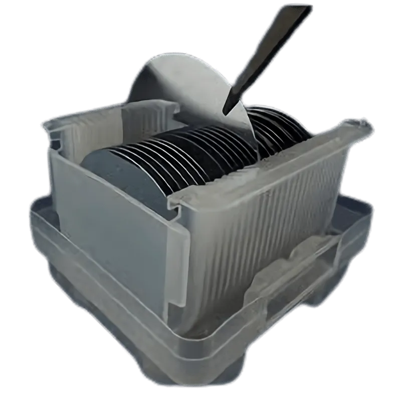
A silicon substrate is the correct default for most semiconductor projects, and an SOI wafer is the upgrade you buy when you need electrical isolation inside the wafer itself rather than on top of it. Everything else, including sapphire and indium phosphide, exists to solve a specific physics problem that silicon cannot. This guide walks through how we choose between them at Soka Technology, what the specs on the product page actually mean, and where a discount code saves you money on the order.
Silicon Substrate vs. SOI Wafer: The Core Difference
A standard silicon substrate is a single-crystal wafer with a uniform bulk. Devices are built into and on top of that bulk, and isolation comes from junctions, trenches, or oxide layers you add during processing.
An SOI wafer, which you will find listed under soi wafer 販売, adds a buried oxide layer between a thin device layer and the handle wafer underneath. That buried oxide does the isolating for you.
| Feature | Silicon substrate | SOI wafer |
|---|---|---|
| Structure | Uniform single crystal | Device layer, buried oxide, handle wafer |
| Isolation | Built during processing | Built into the wafer |
| Best for | Standard CMOS, test structures, teaching, prototyping | Low-power, high-speed, radiation-tolerant, high-temperature devices |
| Cost and lead time | Lower and faster | Higher, fewer stock options |
If you are unsure, start with plain silicon. You can always move to SOI once you know your leakage or speed targets. For current pricing on either, check the latest price on the store page.
When a Plain Silicon Substrate Wins
Most projects do not need SOI, and paying for it adds cost without adding value. We recommend plain silicon when:
- You are prototyping and expect to iterate several times, so you want cheap wafers to burn through.
- Your process already includes well-defined isolation steps you control.
- You need a familiar surface for standard lithography and wet chemistry.
- You are building test structures, calibration samples, or teaching demonstrations.
- You need a specific silicon substrate type, such as a particular doping level or crystal orientation, that is easier to source in bulk silicon.
The related silicon substrate types matter here. Resistivity, doping type, orientation, and thickness all change how your process behaves, so read the spec table rather than assuming a generic wafer will do.
When to Choose an SOI Wafer
We reach for SOI when the buried oxide is doing real work:
- Low-power logic where junction leakage is the limiting factor.
- High-temperature or radiation-exposed environments where latch-up is a risk.
- RF and analog designs that benefit from reduced substrate coupling.
- MEMS work where you want a defined mechanical layer to release.
Availability is the catch. SOI is a smaller market than bulk silicon, so stock is thinner and custom specs take longer. Confirm the device layer thickness and buried oxide thickness before you order, because those two numbers drive everything downstream.
Beyond Silicon: Sapphire and Indium Phosphide Wafers
Some projects should not use silicon at all, and forcing them onto it wastes time.
A sapphire wafer is an insulator, optically transparent, and extremely hard. It suits LED epitaxy, RF filters, and applications needing optical transmission or high thermal and chemical resistance. Sapphire wafer grades differ in surface finish, orientation, and defect density, so grade selection matters more than diameter for many buyers.
An indium phosphide wafer is a compound semiconductor used for high-speed photonics, lasers, and telecommunications devices. It is fragile, expensive, and needs careful handling, but there is no silicon substitute for its bandgap.
A double side polished c sapphire gives you a mirror finish on both faces, which you want for backside alignment, optical paths, or epitaxy where both surfaces matter. Double side polishing also reduces surface roughness and improves thickness uniformity, which shows up in device yield.
Wafer Size, Surface Finish, and the Specs That Matter
Before you request a quote, pin down these four things:
- Diameter. The dimension of 4inch wafer format (100 mm) is the most common compromise between process tooling and cost per device. Larger diameters lower your cost per chip but demand tooling that supports them.
- Surface finish. Single side polished, double side polished, or as-cut. Polished wafers cost more but behave predictably in lithography.
- Thickness and tolerance. Ask for the tolerance, not just the nominal number. Tight tolerance costs more and matters for backside processing.
- Flat or notch, orientation, and doping. These are the specs people forget and then have to reorder.
If a listing shows a paired figure like 100/0.001, read it as two related specs rather than one number, and confirm with the store which is thickness and which is tolerance or resistivity before ordering. Getting that wrong is the most common cause of a returned wafer.
Coated Options: Silver-Coated Silicon Wafers and Silver Silicone Chips
Coated wafers are a shortcut when you need a conductive or reflective surface without running a deposition step yourself.
Silver-coated silicon wafers give you a ready metallized surface for thermal studies, sensor work, or quick electrical contact in test fixtures. Silver silicone chips are the smaller-format companion for bench work, thermal interface trials, and small-area experiments where a full wafer is overkill.
Two cautions. First, silver tarnishes, so store coated parts dry and sealed. Second, coating adhesion depends on the underlying surface prep, so do not assume a coated wafer behaves identically to bare silicon in a high-temperature step.
Buying, Quoting, and Shipping Fragile Wafers
Wafers break in transit more often than they fail in the fab. A few habits keep orders intact:
- Order spares. Buying one extra wafer costs less than a re-order plus shipping.
- Ask how the seller packs. Foam-lined cases with wafer separators are the baseline.
- Inspect on arrival, before you open the inner packaging, and photograph the box.
- Store vertically in a clean, dry place, away from vibration.
On payment, payment options and lead times vary by spec, and custom sizes or coatings usually need a manual quote rather than a checkout click. That is normal. Send the full spec list, including diameter, finish, thickness tolerance, orientation, and quantity, and you will get a usable quote faster.
You can browse the full store overview to see which items are stocked versus made to order, and grab the code before you check out, since the current offer is 10% off all orders.
Who Each Option Suits
- Hobbyist, student, or first prototype: plain silicon substrate in a common 4-inch size, single side polished.
- Low-power or high-temperature device work: SOI wafer with confirmed device and buried oxide thickness.
- Photonics or LED epitaxy: sapphire, double side polished if you need both faces.
- Telecom and laser development: indium phosphide, ordered with spares.
- Thermal or sensor bench work: silver-coated wafers or silver silicone chips.
Pick the material first, then the finish, then the diameter. Doing it in that order avoids the expensive mistake of buying a perfectly good wafer in the wrong material.
 Shopping at Soka Technology? See today's verified Soka Technology discount code
Frequently asked questions
Is a silicon substrate the same as an SOI wafer?
No. A silicon substrate is a uniform single-crystal wafer, while an SOI wafer adds a buried oxide layer between a thin device layer and a handle wafer. That buried oxide provides isolation inside the wafer instead of during processing.
How do I choose between a sapphire wafer and an indium phosphide wafer?
Choose sapphire when you need an insulating, transparent, chemically resistant substrate for LED or RF work. Choose indium phosphide when your device depends on its bandgap, such as lasers and high-speed photonics. They are not interchangeable.
What does the dimension of 4inch wafer mean in practice?
It means a 100 mm diameter wafer. That size balances cost against tooling compatibility for most lab and prototype work, and it is usually the easiest size to find in stock.
Do I need double side polishing?
Only if you work on both faces. Double side polishing helps with backside alignment, optical transmission, and thickness uniformity, but a single side polished wafer is cheaper and fine for standard front-side processing.
Can I use silver-coated silicon wafers in a high-temperature step?
Be careful. Silver tarnishes and coating adhesion depends on the underlying surface preparation, so coated wafers are better suited to bench work, thermal studies, and test fixtures than to aggressive high-temperature processes.
How do I get a quote and discount for fragile wafers?
Send the full spec list including diameter, surface finish, thickness tolerance, orientation, and quantity, since custom specs usually need a manual quote. You can also check the store page for the current discount code before you order.