

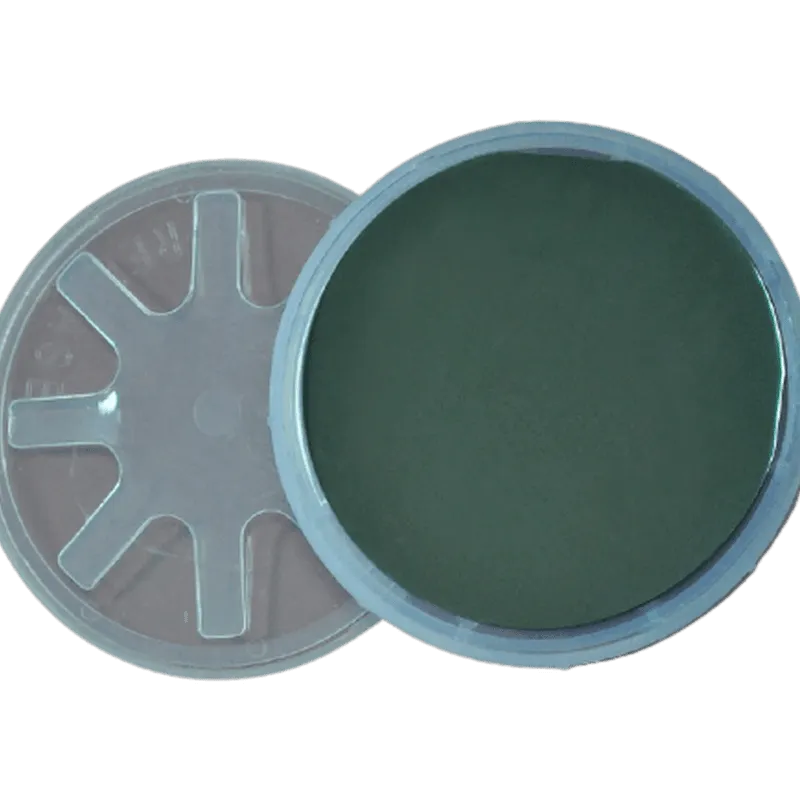
An indium phosphide wafer is the go-to substrate when your design demands high electron mobility, direct bandgap optics, or operation at millimeter-wave frequencies that silicon simply cannot handle. Silicon still dominates volume production for good reason, though. Understanding exactly where each material wins helps you spend your budget where it matters and avoid expensive respins.
What Makes an Indium Phosphide Wafer Different From Silicon
Silicon is an indirect bandgap semiconductor. That means it emits light poorly and tops out at electron mobilities around 1,400 cm²/V·s. An indium phosphide wafer is a III-V compound semiconductor with a direct bandgap, electron mobility above 4,500 cm²/V·s, and a native substrate that lattice-matches key active layers like InGaAsP and InGaAs. Those properties make it the preferred base for:
- Fiber-optic laser diodes and photodetectors (1,310 nm and 1,550 nm windows)
- High-electron-mobility transistors (HEMTs) for 5G and satellite bands
- Solar concentrator cells requiring multi-junction epitaxy
- Terahertz sources and detectors
Silicon, by contrast, wins on cost per wafer, ecosystem maturity, and integration density. If your device is purely digital or runs at low GHz frequencies, the premium of an InP substrate is hard to justify.
Silicon Substrate Types and When to Use Them
Not all silicon is the same, and Soka Technology's silicon substrate catalog reflects that diversity. Key variables that drive your selection include:
- Orientation: (100) for CMOS, (111) for certain power and RF devices
- Resistivity: Standard versus high-resistivity for RF isolation
- Surface finish: Single-side polished for most epitaxy; double-side polished for through-wafer optics or lithography on both faces
For applications needing a buried oxide layer, the soi wafer 販売 (silicon-on-insulator) adds a thin silicon film above SiO₂, dramatically reducing parasitic capacitance for RF and low-power logic.
| Substrate | Key Advantage | Typical Application |
|---|---|---|
| Bulk silicon | Low cost, mature process | CMOS, MEMS, power devices |
| SOI | Low parasitics, isolation | RF switches, low-power logic |
| Indium phosphide | High mobility, direct bandgap | Photonics, mmWave, HEMTs |
| Sapphire | Electrical isolation, UV transparency | GaN-on-sapphire, optics |
Sapphire and Coated Wafers: Rounding Out the Options
Sapphire substrates occupy a niche between silicon and compound semiconductors. The double side polished c sapphire from Soka Technology offers high hardness, wide bandgap electrical isolation, and excellent UV-to-IR transparency, making it the standard carrier for GaN epitaxy in blue LEDs and power HEMTs. The sapphire wafer range covers multiple orientations and grades to match your specific surface finish choices.
For experimental or sensor work, coated wafers add functionality without full compound substrate cost:
- Silver-coated silicon wafers: Reflective surface for SERS, plasmonics, and calibration standards
- Silver silicone chips: Pre-diced coated chips for smaller-scale sensor or optics work
These coated options let research teams validate concepts at lower cost before committing to InP or sapphire runs.
Wafer Size Options and Surface Finish Choices
Wafer size options directly affect yield per run, tool compatibility, and price. Soka Technology supplies substrates from small research diameters up through production formats. If you are qualifying a 100 mm process, the dimension of 4inch wafer listing gives you the spec sheet and pricing for that node. For precision resistivity-controlled material, the 100/0.001 product page details ultra-low resistivity silicon used in calibration and advanced sensor work.
Surface finish choices matter at every step:
- Single-side polished (SSP): Standard for most epitaxial growth; cheaper
- Double side polishing: Required when back-side lithography, bonding, or through-wafer vias are part of your process flow
- Epi-ready: Cleaned and packaged to minimize surface contamination ahead of deposition
For InP specifically, epi-ready finish is almost always specified because the surface degrades quickly in ambient air. Order in packaging that keeps the surface under nitrogen until you are ready to load.
Practical Guidance: Requesting a Quote and Ordering
Soka Technology operates as a specialty supplier, so most compound and sapphire wafer grades are quote-based rather than fixed-price. Here is how to streamline your request:
- Specify orientation and conductivity type (n-type Fe-doped semi-insulating is the most common for InP)
- State diameter and thickness tolerance (for example, 50 mm, 350 µm ± 25 µm)
- Confirm surface finish (SSP epi-ready vs. double side polished)
- Give your target quantity and lead time so the team can source or cut to order
Shipping fragile wafers over long distances is a real concern. InP is brittle; request individual wafer carriers or cassette packaging and confirm whether the supplier uses foam-lined double-box methods. Soka Technology's listings note packaging details, so check each product page before you finalize.
Before you submit your order, grab the discount code for 10% off all orders, which meaningfully reduces cost on higher-ticket compound substrates.
Choosing the Right Substrate for Your Project
Use this quick decision framework:
- High-volume digital or MEMS: silicon substrate or SOI
- RF/photonics above 10 GHz or laser epitaxy: indium phosphide wafer
- GaN power or blue-light devices: double side polished c sapphire or sapphire wafer
- Plasmonic or sensor research on a budget: silver-coated silicon wafers
No single substrate is universally best. The right answer comes from matching material properties to your device physics, then balancing that against wafer cost and process compatibility. Check the latest pricing and coupon at Soka Technology before you lock in your substrate selection, especially for compound and coated wafers where prices can shift with availability.
 Shopping at Soka Technology? See today's verified Soka Technology discount code
Frequently asked questions
What is an indium phosphide wafer typically used for?
An indium phosphide wafer is primarily used for photonic devices operating in the 1,310 nm and 1,550 nm fiber-optic windows, high-electron-mobility transistors for 5G and satellite frequencies, and multi-junction solar cells. Its direct bandgap and high electron mobility make it unsuitable to replace with silicon in these applications.
How does InP compare to sapphire as an epitaxial substrate?
Indium phosphide is used as a native substrate for III-V epitaxial layers that lattice-match InP, while sapphire is an insulating oxide used mainly for GaN-based devices like LEDs and power transistors. They serve different device families and are rarely interchangeable for the same application.
When should I choose a double side polished wafer over single-side polished?
Choose double side polishing when your process requires back-side lithography, through-wafer vias, wafer bonding, or any optical access from both faces. Single-side polished is sufficient and more cost-effective for standard front-side-only epitaxy and device fabrication.
Can I order a silicon substrate and an indium phosphide wafer from the same supplier?
Yes. Soka Technology stocks both silicon substrates and compound semiconductor wafers, allowing you to source multiple material types under one order and potentially apply a single discount code to the whole cart.
What wafer sizes does Soka Technology offer?
Soka Technology offers a range of wafer size options from small research-grade diameters up through production formats such as 4-inch (100 mm). Check individual product pages for exact diameter, thickness, and tolerance specifications, as compound wafer sizes may differ from standard silicon formats.
How should fragile compound wafers like InP be shipped to avoid breakage?
Shipping fragile wafers like InP safely requires individual wafer carriers or cassette trays inside foam-lined double-walled boxes, ideally under nitrogen or dry-air atmosphere to protect the epi-ready surface. Always confirm the supplier's packaging method before placing a large order.