

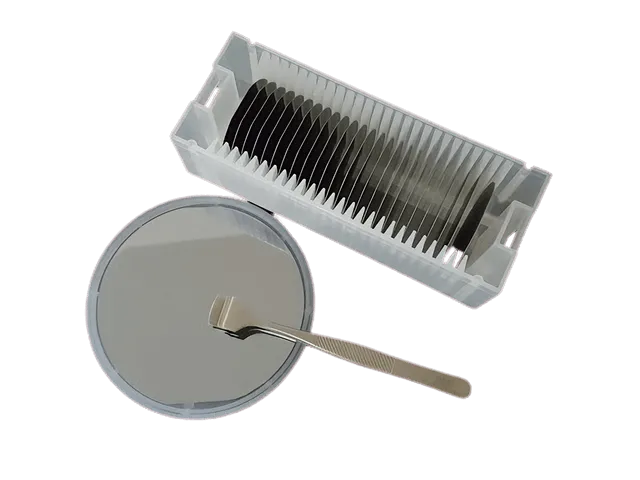
Double side polished c sapphire substrates are among the most demanding materials to handle in a semiconductor or photonics lab, and a single contamination event or mechanical shock can compromise an entire batch. Soka Technology supplies research- and production-grade double side polished c sapphire alongside a wide range of companion substrates, including sapphire wafer variants, silicon substrate options, and indium phosphide wafer stock. This guide covers everything you need to know about surface finish choices, safe handling, storage best practices, and how to pick the right substrate for your application.
What Makes Double Side Polished C Sapphire Different
Standard sapphire wafers are polished on one face only. Double side polishing (DSP) removes saw damage and sub-surface stress from both the front and back surfaces, giving you:
- Two optically flat faces suitable for transmission measurements or backside processing
- Tighter total thickness variation (TTV) critical for lithography alignment
- Lower warp and bow compared to single-side polished equivalents
- C-axis orientation (0001), the most common cut for GaN epitaxy and LED manufacturing
If your process involves double-sided lithography, IR or UV transmission windows, or high-temperature annealing where bow matters, DSP c-plane sapphire is the correct choice. Single-side polished sapphire wafer stock remains the right pick for simpler epi applications where backside finish is irrelevant.
Sapphire Wafer Grades and Surface Finish Choices
Not all sapphire substrates ship in the same condition. When reviewing Soka Technology's listings, pay attention to these grade indicators:
| Grade | Surface Finish | Typical Ra | Best Use |
|---|---|---|---|
| Epi-ready | DSP + chemical clean | < 0.3 nm | GaN / LED epi |
| Optical | DSP + AR coat option | < 0.5 nm | Windows, optics |
| Research | SSP or DSP | < 1.0 nm | General R&D |
| As-cut | Lapped only | > 10 nm | Dicing feedstock |
Epi-ready and optical grades ship individually wrapped and are the most sensitive to mishandling. Research and as-cut grades tolerate slightly less stringent conditions but still require clean-room protocols on receipt.
Handling Double Side Polished C Sapphire Safely
Sapphire ranks 9 on the Mohs scale, so scratching it takes real effort, but the polished surfaces are highly susceptible to particulate contamination and fingerprints that are nearly impossible to remove without re-polishing.
Essential handling rules:
- Always use ESD-safe, powder-free nitrile or latex gloves before touching any substrate
- Pick up wafers with vacuum wands or Teflon-tipped tweezers at the edge only; never grip the polished face
- Work over a cleanroom-grade wipe or gel mat to cushion accidental contact
- Inspect under oblique lighting (a bright LED at a low angle) before and after transfer to catch haze or particles
- If a particle lands on the surface, use nitrogen gun blowoff first; liquid cleaning is a last resort
For compound wafers like indium phosphide wafer stock, the same edge-only rule applies, but InP is far more brittle (cleavage planes) so wand pressure must be even lighter.
Storage Best Practices for Polished Wafers
Improper storage degrades a pristine surface faster than handling errors do. Follow these guidelines to protect your investment between process steps.
Short-term (days to weeks):
- Store individually in nitrogen-purged wafer carriers or sealed cassettes
- Keep carriers in a desiccated, dark enclosure at 15-25 °C
- Never stack bare wafers face-to-face or face-to-back without separator tissue
Long-term (months):
- Vacuum-seal individual wafers in anti-static poly bags with a silica desiccant sachet
- Label the bag with orientation flat / notch position before sealing so you do not need to open it to identify the wafer
- Log the date; even inert sapphire can adsorb organic contaminants from ambient air over extended periods
The same storage logic applies to silicon substrate and silver-coated silicon wafers in your inventory. Coated surfaces are especially prone to tarnish if left exposed, so sealed storage is non-negotiable for silver-coated stock.
Sizing, Specs, and Ordering the Right Substrate
Before placing an order, confirm these four parameters:
- Diameter - Soka Technology lists common semiconductor wafer sizes; the dimension of 4inch wafer product page is a useful reference for standard tolerances across substrate types
- Thickness - DSP wafers have tighter thickness specs than SSP; check the datasheet for TTV limits
- Orientation - C-plane (0001) is standard for most LED and RF applications; other cuts (R, A, M) are available on request
- Quantity - Small research orders (single wafers) and production lots are both supported; use the quote request form for volume pricing
If your project also requires exotic compound substrates, the indium phosphide wafer listings carry orientation, carrier concentration, and polish details directly in the product spec. For specialty coated materials, silver silicone chips round out the catalog for sensor and MEMS applications.
You can check the latest pricing and grab the current 10% off code before adding items to your cart.
Shipping Fragile Wafers: What to Expect
Soka Technology ships wafers in rigid plastic cassettes or individual gel-pak carriers, surrounded by foam-lined boxes. Here is what to do on receipt:
- Inspect the outer box for crush damage before signing for the shipment
- Open at room temperature if the package has been in a cold vehicle; allow 30 minutes for thermal equilibration before exposing wafers to avoid condensation
- Check the packing slip against your order spec (diameter, orientation, polish, quantity)
- Photograph any damage immediately and contact the supplier before disturbing the contents
Fragile substrate shipping is especially relevant for DSP stock because the unprotected backside is just as polished and vulnerable as the front.
Comparing Key Substrate Options at Soka Technology
If you are deciding between substrate types for a new project, this quick comparison covers the most popular materials in the catalog:
| Substrate | Key Strength | Typical Application |
|---|---|---|
| double side polished c sapphire | Optically clear, chemically inert, high hardness | GaN epi, UV/IR windows, RF filters |
| silicon substrate | Low cost, mature process ecosystem | CMOS, MEMS, general epi |
| indium phosphide wafer | Direct bandgap, high electron mobility | Lasers, photonic ICs, solar |
| soi wafer 販売 | Buried oxide for isolation | RF SOI, low-power CMOS |
| silver-coated silicon wafers | Reflective / conductive surface layer | Sensor packages, SERS substrates |
For teams running GaN-on-sapphire or similar heteroepitaxy processes, double side polished c sapphire remains the dominant platform. Silicon and InP fill the gaps where cost or electronic properties take priority.
Requesting a Quote and Using a Discount Code
Soka Technology accepts custom orders for non-standard diameters, orientations, and coatings. To request a quote, use the contact form on the product listing page and include your required diameter, thickness, orientation, polish type, quantity, and any certification requirements (SEMI standard, COA, etc.).
For standard in-stock items, pricing is listed directly on the product pages. Before checkout, grab the current discount code at our Soka Technology coupon page to save on your order. The code applies site-wide, so it works equally well whether you are ordering a single research wafer or a full cassette for production use.
 Shopping at Soka Technology? See today's verified Soka Technology discount code
Frequently asked questions
What does 'double side polished c sapphire' mean in a product spec?
It means the sapphire substrate has been mechanically and chemically polished on both the front and back faces, with the crystal oriented along the c-axis (0001 plane). This gives you two optically flat, low-roughness surfaces and tighter thickness uniformity compared to single-side polished wafers.
Can I clean a polished sapphire wafer if it gets contaminated?
Yes, but the method depends on the contaminant. Particulates should be removed with dry nitrogen blowoff first. Organic residues typically respond to a standard RCA-1 clean (NH4OH/H2O2/H2O). Avoid abrasive wipes or strong acids that could micro-scratch the polished surface.
How does sapphire compare to a silicon substrate for GaN epitaxy?
Sapphire is the preferred platform for GaN LED and RF applications because its thermal and chemical stability at high epi temperatures outweighs the lattice mismatch penalty. Silicon substrates are lower cost and larger in diameter but require complex buffer layer engineering to manage the greater lattice and thermal mismatch with GaN.
What wafer sizes does Soka Technology carry for sapphire substrates?
Soka Technology offers sapphire substrates in common semiconductor wafer sizes. Check the dimension of 4inch wafer product page for standard size tolerances, and use the quote form for non-standard or larger diameters.
Is there a discount code available for Soka Technology orders?
Yes. You can find the current active code on our Soka Technology coupon page, which lists the latest offer for all orders site-wide including sapphire, silicon, and indium phosphide wafers.
How should I store indium phosphide wafers alongside sapphire substrates?
Both materials should be stored individually in nitrogen-purged or vacuum-sealed carriers with desiccant, away from light and temperature swings. InP is more brittle than sapphire and also oxidizes more readily, so sealed anti-static bags are especially important for long-term InP storage.